

Temperature Compensated Crystal Oscillators (TCXO5032) PTC5032

Features
Temperature Compensated Crystal Oscillators PTC5032
Low voltage operation
Low phase noise
Single packaged structure
Prevention of moisture packing is unnecessary
Moisture sensitivity level: LEVEL 1 (IPC/ JEDC J-STD-033)
TCXO in ceramic seam seal SMD packages - HCMOS/ LVCMOS output
Applications
Mobile phone (W-CDMA, CDMA2000, TD-SCDMA, GSM, GPRS, Mobile W-PHS)
Type :
AT5Model :
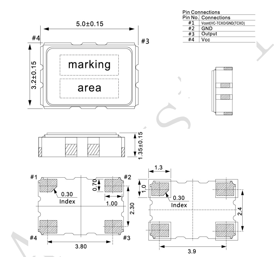
PTC5032Package size :
5.0*3.2*1.35mmFrequency :
9.600M~52.000MTemperature Compensated Crystal Oscillators (TCXO5032) PTC5032
This product is a 5.0x 3.2mm size temperature compensated crystal oscillator (TCXO), suitable for providing stable clock signals to microcontrollers, processors and digital systems. Its main features include low voltage operation, low phase noise and single package structure. The oscillator is suitable for applications such as mobile phones, wireless communications, GPS, etc., with high frequency stability, low power consumption and good temperature compensation performance. The product adopts HCMOS/LVCMOS output and complies with RoHS and REACH standards.
1. ELECTRICAL SPECIFICATIONS
| No. | Item | Electrical Specification | Remark | |||
| Min. | Type | Max. | Units | |||
| 1 | Nominal Frequency | 9.6~52.000 | MHz | |||
| 2 | Nominal Frequency Tolerance | -2.0 | - | +2.0 | ppm | Frequency at 25℃ , 1 hour after reflow |
| 3 | Frequency Stability Over Temperature | -0.5 | - | +0.5 | ppm | Referenced to the Frequency at 25℃ . |
| 4 | Storage Temperature Range | -20 | - | +70 | ℃ | The operating temperature range over which the frequency stability is measured |
| 5 | Frequency Slope of Perturbations | -0.3 | - | +0.3 | ppm/ ℃ | Minimum of 1 frequency reading every 2℃ , over -40℃ to +85℃ |
| 6 | Supply Voltage Stability | -0.3 | - | +0.3 | ppm/ ℃ | Supply voltage varied ±5% at 25 ℃ |
| 7 | Load Sensitivity | -0.2 | - | +0.2 | ppm | ±10% load change |
| 8 | Aging | -1.0 | - | +1.0 | ppm | first year at 25 ℃ |
| 9 | Supply Voltage | 1.8 | - | 3.3 | v | |
| 10 | Current Consumption | - | - | 2.0 | mA | At maximum supply voltage |
| 11 | Output Waveform | Clipped sine wave | DC Coupled clipped sine wave | |||
| 12 | Output Voltage Level | 0.8 | - | 2 | Vp-p | |
| 13 | Output Load | 10Kohm//10Pf | ||||
| 14 | StartUp Time | - | - | 2 | ms | |
| 15 | Pin 1, tri-state function | pin 1=H or open. output active at pin 3 pin 1=L. high impedance at pin 3 |
||||
| 16 | Package type | 5.0*3.2*1.35 | ||||
2. Dimension (Unit: mm)
3.For more FAQs and other services, please click on the image below to view.


Features Low voltage operation Low phase noise Prevention of moisture packing is unnecessary Moisture sensitivity level: LEVEL 1 (IPC/ JEDC J-STD-033) Applications Mobile phone (W-CDMA, CDMA2000, TD-SCDMA, GSM, GPRS, Mobile W-PHS) Other wireless radio communications GPS Industrial radio communications Wearable devices
Read More
Features Low voltage operation Low phase noise Single packaged structure Prevention of moisture packing is unnecessary Moisture sensitivity level: LEVEL 1 (IPC/ JEDC J-STD-033) Applications Mobile phone (W-CDMA, CDMA2000, TD-SCDMA, GSM, GPRS, Mobile W-PHS) Other wireless radio communications(WIMAX) GPS
Read More
Features Low voltage operation Low phase noise Single packaged structure Prevention of moisture packing is unnecessary Moisture sensitivity level: LEVEL 1 (IPC/ JEDC J-STD-033) 2.0*1.6mm seam seal SMD packages - HCMOS/ LVCMOS output Applications Mobile phone (W-CDMA, CDMA2000, TD-SCDMA, GSM, GPRS, Mobile W-PHS), other wireless radio communications(WIMAX), GPS
Read More
Features Temperature Compensated Crystal Oscillators PTC5032 Low voltage operation Low phase noise Single packaged structure Prevention of moisture packing is unnecessary Moisture sensitivity level: LEVEL 1 (IPC/ JEDC J-STD-033) TCXO in ceramic seam seal SMD packages - HCMOS/ LVCMOS output Applications Mobile phone (W-CDMA, CDMA2000, TD-SCDMA, GSM, GPRS, Mobile W-PHS)
Read More
Features Ultra smaller size Low operation voltage Low jitter Low standby current Low current consumption
Read More


 IPv6 network supported