Temperature Compensated Crystal Oscillators (TCXO3225) PTC3225
Features
Low voltage operation
Low phase noise
Single packaged structure
Prevention of moisture packing is unnecessary
Moisture sensitivity level: LEVEL 1 (IPC/ JEDC J-STD-033)
Applications
Mobile phone (W-CDMA, CDMA2000, TD-SCDMA, GSM, GPRS, Mobile W-PHS)
Other wireless radio communications(WIMAX)
GPS
Type :
AT3Model :
PTC3225Package size :
3.2*2.5*0.9mmFrequency :
9.600M~52.000MTemperature Compensated Crystal Oscillators (TCXO3225) PTC3225
Temperature Compensated Crystal Oscillators PTC3225
TCXO oscillator in ceramic seam seal SMD packages - HCMOS/ LVCMOS output
A-Crystal PTC3225 is a 3.2x 2.5mm temperature compensated crystal oscillator (TCXO) in a ceramic sealed SMD package with HCMOS/LVCMOS output. The crystal oscillator has the characteristics of low voltage operation and low phase noise, and is suitable for a variety of application scenarios such as mobile phones, wireless communications, and GPS.
1. ELECTRICAL SPECIFICATIONS
| No. | Item | Electrical Specification | Remark | |||
| Min. | Type | Max. | Units | |||
| 1 | Nominal Frequency | 9.6~52.000 | MHz | |||
| 2 | Nominal Frequency Tolerance | -2.0 | - | +2.0 | ppm | Frequency at 25℃ , 1 hour after reflow |
| 3 | Frequency Stability Over Temperature | -0.5 | - | +0.5 | ppm | Referenced to the Frequency at 25℃ . |
| 4 | Storage Temperature Range | -20 | - | +70 | ℃ | The operating temperature range over which the frequency stability is measured |
| 5 | Frequency Slope of Perturbations | -0.3 | - | +0.3 | ppm/ ℃ | Minimum of 1 frequency reading every 2℃ , over -40℃ to +85℃ |
| 6 | Supply Voltage Stability | -0.3 | - | +0.3 | ppm/ ℃ | Supply voltage varied ±5% at 25 ℃ |
| 7 | Load Sensitivity | -0.2 | - | +0.2 | ppm | ±10% load change |
| 8 | Aging | -1.0 | - | +1.0 | ppm | first year at 25 ℃ |
| 9 | Supply Voltage | 1.8 | - | 3.3 | v | |
| 10 | Current Consumption | - | - | 2.0 | mA | At maximum supply voltage |
| 11 | Output Waveform | Clipped sine wave | DC Coupled clipped sine wave | |||
| 12 | Output Voltage Level | 0.8 | - | 2 | Vp-p | |
| 13 | Output Load | 10Kohm//10Pf | ||||
| 14 | StartUp Time | - | - | 2 | ms | |
| 15 | Pin 1, tri-state function | pin 1=H or open. output active at pin 3 pin 1=L. high impedance at pin 3 |
||||
| 16 | Package type | 3.2*2.5*0.9 | ||||
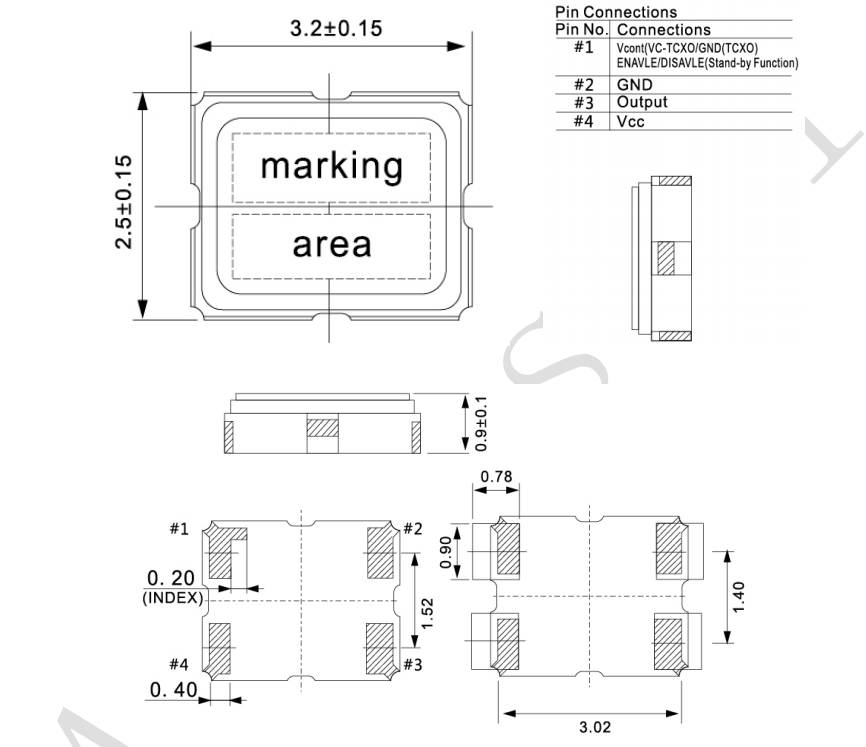
2. Dimension (Unit: mm)

3.For more FAQs and other services, please click on the image below to view.