

Features
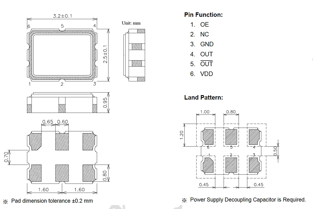
3225 SMD Crystal Oscillator with 6pad
Supply Voltage: 1.8V/2.5V/2.8V/3.OV/3.3V/5.0V.
Tri-state function
Low current consumption CMOS Level Output
High speed start-up: 2ms max. until frequency output after power [Standard] Frequency tolerance: ±35x 10-6 and below (-40~+85°C, includes frequency tolerance at room temperature
Frequency tolerance at room temperature: ±11x10-6 and below (Accuracy ±30 sec/month)
AEC-Q 100 compliant
Applications
Timer module, Industrial measuring equipment
Consumer Product, Clock source for RTC automotive multimedia device
Type :
AOAModel :
POSC3225JPackage size :
3.2*2.5*0.95mmFrequency :
25.000M~320.000MSMD Crystal Oscillators POSC3225J (6PAD)
The 3225 SMD Crystal Oscillators is an environmentally friendly active oscillator that is seam sealed in a package, and it could deliver satisfying performance in a safe and reliable manner.
As a stand alone clock generator, this electronic device exhibits a broad frequency range, from 25.000MHZ to 32.000MHz,and its supply voltage is 1.8V, 2.5Vor 3.3V. Moreover, our surface
mount crystal oscillator is also characterized by CMOS output, tri-state function, low phase noise and ultra small size, making it applicable for space vehicles, mobile communication devices,
communication base stations, etc.
1. ELECTRICAL SPECIFICATIONS
| No. | Item | Symb | Electrical Specification | Remark | |||
| Min. | Type | Max. | Units | ||||
| 1 | Nominal Frequency | F0 | 25.000 | 320.000 | MHz | |
|
| 2 | Frequency Stability | ST | ±25 | ±100 | ppm | |
|
| 3 | Operating Temperature Range | TOPR | -20 | 125 | ℃ | |
|
| 4 | Storage Temperature Range | TSTG | -55 | 125 | ℃ | |
|
| 5 | Power supply Voltage | VDD | 2.5 | 3.3 | V | ±5% | |
| 6 | Start UP Time | TOSC | 10 | ms | To 90% of Final Amplitude | ||
| 7 | Output waveform | LVDS Electrical Characteristics | |||||
| 8 | Current Consumption | ICC | 60 | mA | RL=50 Ω to VDD -2V | ||
| 9 | Standby current | ICC | 30 | uA | OE=LOW | ||
| 10 | Output Voltage High | VOH | 1.43 | 1.6 | V | |
|
| 11 | Output Voltage Low | VOL | 0.9 | 1.1 | V | |
|
| 12 | Rise Time | Tr | 0.5 | 1.0 | ns | 20% ~ 80% Output Swing | |
| 13 | Time Fall | Tf | 0.5 | 1.0 | ns | 80% ~ 20% Output Swing | |
| 14 | Symmetry | TH/T | 45 | 50 | 55 | % | |
| 15 | Enable Voltage High | 0.7vDD | v | Note 2, (Logic 1) | |||
| 16 | Enable Voltage Low | 0.3vDD | v | Note 2, (Logic 0) | |||
| 17 | Output Enable Delay Time | 2 | ms | |
|||
| 18 | Output Disable Delay Time | 200 | ns | |
|||
| 19 | Output waveform | LVPECL Electrical Characteristics | |||||
| 20 | Current Consumption | ICC | 80 | mA | RL=50 Ω to VDD -2V | ||
| 21 | Standby current | ICC | 10 | uA | OE=LOW | ||
| 22 | Output Voltage High | VOH | vDD-1.025 | vDD-0.88 | V | |
|
| 23 | Output Voltage Low | VOL | vDD-1.81 | vDD-1.62 | V | |
|
| 24 | Rise Time | Tr | 0.5 | 1.0 | |
20% ~ 80% Output Swing | |
| 25 | Time Fall | Tf | 0.5 | 1.0 | ns | 80% ~ 20% Output Swing | |
| 26 | Symmetry | TH/T | 45 | 50 | 55 | % | |
| 27 | Enable Voltage High | 0.7vDD | v | Note 2, (Logic 1) | |||
| 28 | Enable Voltage Low | 0.3vDD | v | Note 2, (Logic 0) | |||
| 29 | Output Enable Delay Time | 2 | ms | ||||
| 30 | Output Disable Delay Time | 200 | ns | ||||
| 31 | Output waveform | HCSL Electrical Characteristics | |||||
| 32 | Current Consumption | ICC | 40 | mA | RL=50 Ω to VDD -2V | ||
| 33 | Standby current | ICC | 10 | uA | OE=LOW | ||
| 34 | Output Voltage High | VOH | 660 | 740 | 850 | mV | |
| 35 | Output Voltage Low | VOL | -150 | 0 | 150 | mV | |
| 36 | Rise Time | Tr | 0.5 | 1.0 | ns | 20% ~ 80% Output Swing | |
| 37 | Time Fall | Tf | 0.5 | 1.0 | ns | 80% ~ 20% Output Swing | |
| 38 | Symmetry | TH/T | 45 | 50 | 55 | % | |
| 39 | Enable Voltage High | 0.7vDD | v | Note 2, (Logic 1) | |||
| 40 | Enable Voltage Low | 0.3vDD | v | Note 2, (Logic 0) | |||
| 41 | Output Enable Delay Time | 2 | ms | ||||
| 42 | Output Disable Delay Time | 200 | ns | ||||
| 43 | Package type | 3.2*2.5*0.95 | |||||
2. Dimension (Unit: mm)

3.For more FAQs and other services, please click on the image below to view.


Features 1612 size, 0.5mm high. Ultra miniature and lightweight SMD SPXO 3-state function EC-Q 100compliant Supply Voltage: 1.8V/ 2.5V/ 2.8V/ 3.0V/ 3.3V Available frequency range: 0.584375~80MHz SMD crystal oscillator is available up to 80MHz by using AT cut fundamental resonator Low jitter provides for high performance Applications PC, PDA, PND, DSC, DVD, DVC, HDD Smartphone, WiLAN, WiMAX, Bluetooth PC peripherals gaming equipment Wearable devices
Read More
Features 2016 size. Ultra miniature and lightweight SMD SPXO 3-state function EC-Q 100compliant Supply Voltage: 1.8V/ 2.5V/ 2.8V/ 3.0V/ 3.3V Available frequency range: 0.584375~80MHz Available up to 80MHz by using AT cut fundamental resonator Low jitter provides for high performance Applications PC, PDA, PND, DSC, DVD, DVC, HDD Smartphone, WiLAN, WiMAX, Bluetooth PC peripherals gaming equipment Wearable devices
Read More
Features Typical 2.5×2.0×0.85 mm ceramic SMD crystal oscillator, 2520 size. Ultra miniature and lightweight SMD SPXO 3-state function(Tri-state enable/disable) EC-Q 100 compliant Supply Voltage: 1.8V/ 2.5V/ 2.8V/ 3.0V/ 3.3V Available frequency range: 32.768KHZ~125.000MHz Available up to 80MHz by using AT cut fundamental resonator Low jitter provides for high performance tight symmetry(45 to 55%)available Applications PC, PDA, PND, DSC, DVD, DVC, HDD, Smartphone, WiLAN, WiMAX, Bluetooth, PC peripherals gaming equipment, wearable devices
Read More
Features Typical 2.5×2.0×0.85 mm ceramic SMD crystal oscillator, 2520 size with 6pad Ultra miniature and lightweight SMD SPXO 3-state function(Tri-state enable/disable) EC-Q 100 compliant Supply Voltage: 1.8V/ 2.5V/ 2.8V/ 3.0V/ 3.3V Available frequency range: 32.768KHZ~125.000MHz Available up to 80MHz by using AT cut fundamental resonator Low jitter provides for high performance tight symmetry(45 to 55%)available Applications PC, PDA, PND, DSC, DVD, DVC, HDD, Smartphone, WiLAN, WiMAX, Bluetooth, PC peripherals gaming equipment, wearable devices
Read More
Features Supply Voltage: 1.8V/2.5V/2.8V/3.OV/3.3V/5.0V.Tri-state function Low current consumption CMOS Level Output High speed start-up: 2ms max. until frequency output after power [Standard] Frequency tolerance: ±35x 10-6 and below (-40~+85°C, includes frequency tolerance at room temperature Frequency tolerance at room temperature: ±11x10-6 and below (Accuracy ±30 sec/month) AEC-Q 100 compliant Applications Timer module, Industrial measuring equipment Consumer Product, Clock source for RTC automotive multimedia device
Read More
Features Low current consumption 3-state function availble General purpose +5.0V HCMOS crystal oscillators Miniature Hermetically Sealed package Optimized characteristic for single gate drive/lower Loading conditions RoHS and REACH Compliant. Applications PC, Peripherals, Visual, FA equipment applications, Graphics and Multimedia A/V Clock Applications as well as Bluetooth, MPEG and HDTV Clocks
Read More
Features 3225 SMD Crystal Oscillator with 6pad Supply Voltage: 1.8V/2.5V/2.8V/3.OV/3.3V/5.0V. Tri-state function Low current consumption CMOS Level Output High speed start-up: 2ms max. until frequency output after power [Standard] Frequency tolerance: ±35x 10-6 and below (-40~+85°C, includes frequency tolerance at room temperature Frequency tolerance at room temperature: ±11x10-6 and below (Accuracy ±30 sec/month) AEC-Q 100 compliant Applications Timer module, Industrial measuring equipment Consumer Product, Clock source for RTC automotive multimedia device
Read More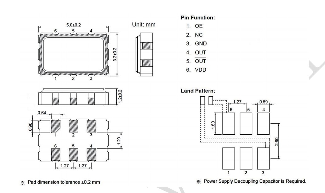
Features 5032 SMD Crystal Oscillator with 6pad Low current consumption 3-state function availble General purpose +5.0V HCMOS crystal oscillators Miniature Hermetically Sealed package Optimized characteristic for single gate drive/lower Loading conditions RoHS and REACH Compliant. Applications PC, Peripherals, Visual, FA equipment applications, Graphics and Multimedia A/V Clock Applications as well as Bluetooth, MPEG and HDTV Clocks
Read More


 IPv6 network supported